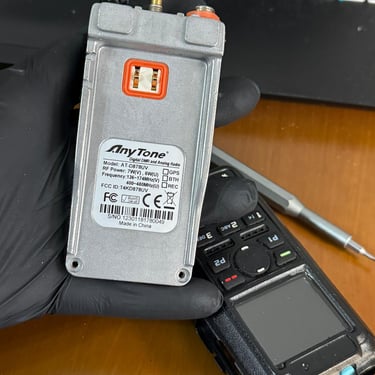
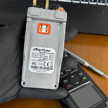
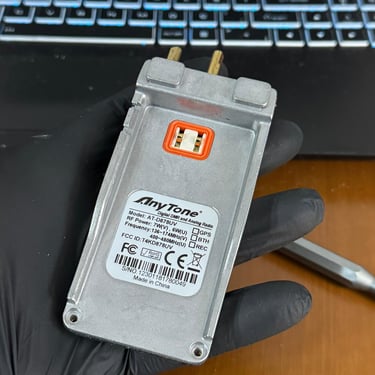
Anytone AT-D878UV (Version 1) Hardware Teardown and Technical Analysis
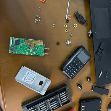
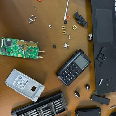
This article presents a detailed hardware teardown and RF architecture analysis of the Anytone AT-D878UV Version 1 DMR/Analog handheld transceiver. The evaluation is based on direct inspection of the main PCB after disassembly, focusing on RF signal paths, baseband processing, power management, and mechanical layout.
AYBERK BLOG
Anytone AT-D878UV (Version 1) Hardware Teardown and Technical Analysis
Introduction
This article presents a detailed hardware teardown and RF architecture analysis of the Anytone AT-D878UV Version 1 DMR/Analog handheld transceiver. The evaluation is based on direct inspection of the main PCB after disassembly, focusing on RF signal paths, baseband processing, power management, and mechanical layout.
The AT-D878UV V1 is a dual-band (VHF/UHF) handheld radio supporting both analog FM and DMR Tier II digital modulation.
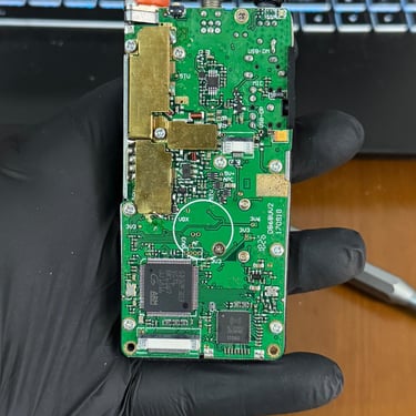
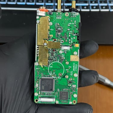
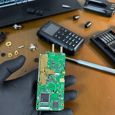
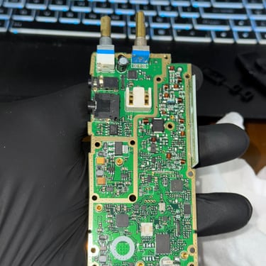
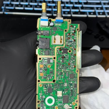
PCB Layout and Layer Structure
The main PCB is a high-density, multi-layer board (estimated 6–8 layers) populated with fine-pitch SMD components. The board can be logically divided into the following functional areas:
Upper section: RF front-end and antenna interfaces
Middle section: IF, filtering, and RF control circuitry
Lower section: Baseband processor, memory, and power management
Extensive ground planes and carefully routed RF traces indicate a design optimized for signal integrity and EMI suppression.
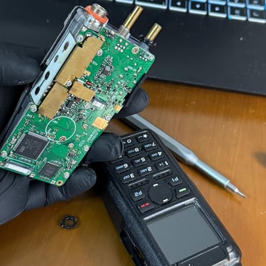
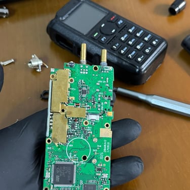
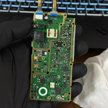
Antenna Interface and RF Front-End
At the top of the PCB, the antenna connection and RF switching network are located. This section includes:
TX/RX antenna switching circuitry
Band-pass and low-pass filters
RF chokes and impedance matching networks
Discrete inductors and RF-grade ceramic capacitors suggest separate optimization for the VHF (136–174 MHz) and UHF (400–480 MHz) bands, enabling efficient dual-band operation using a single antenna port.
Receiver (RX) Signal Chain
The receiver architecture follows the general signal flow:
Antenna → RF Filter → LNA → Mixer → IF → ADC
The observed RF ICs and surrounding passive components indicate a low-IF or superheterodyne design. Digital IF processing is handled either by the main baseband processor or an integrated RF transceiver IC.
Design priorities in this stage include:
Low noise figure
Image rejection
Symbol accuracy required for DMR demodulation
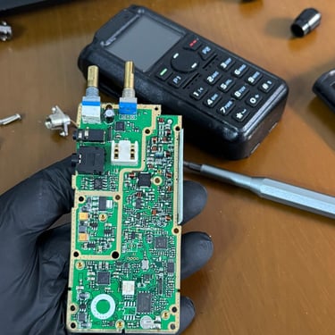
Transmitter (TX) and Power Amplifier Stage
On the transmit side, the signal path can be summarized as:
DSP/Modulator → Driver Amplifier → Power Amplifier → Harmonic Filter → Antenna
A dedicated PA device is supported by:
Bias control circuitry
Extensive copper pours for heat spreading
Thermal vias for heat dissipation
This design supports typical handheld output power levels (approximately 5–7 W), particularly critical in the UHF band. LC-based output filtering provides effective harmonic suppression.
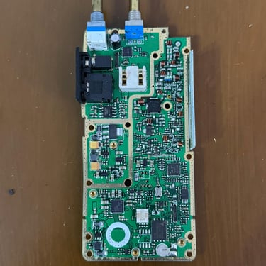
Baseband Processor and DMR Infrastructure
The lower section of the PCB hosts the main MCU/baseband processor responsible for:
DMR protocol handling
AMBE+2 vocoder control
Analog FM audio processing
Management of CPS-defined parameters
External Flash memory stores:
Channel configurations
Codeplug data
User and system settings
Power Management Architecture
Powered by a Li-ion battery, the radio employs a multi-stage power regulation system:
High-efficiency buck converters
Low-noise LDO regulators for RF and digital isolation
A dedicated high-current supply path for the PA stage
This architecture minimizes voltage sag during transmission and prevents PA-induced noise from affecting sensitive digital circuits.
Relationship Between the EW1EM Preset and Hardware Behavior
Although CPS presets do not directly modify hardware, the EW1EM preset influences radio performance through parameters such as:
TX deviation levels (FM and DMR)
RX/TX gain balance
Audio DSP characteristics
RF power level configuration
These parameters are tuned with awareness of the underlying RF and baseband architecture, resulting in improved on-air performance.
Conclusion
The Anytone AT-D878UV Version 1 demonstrates a mature and well-engineered design, with clear separation between RF and digital domains, robust power handling, and effective EMI mitigation. The internal architecture explains the radio’s stable performance in both analog FM and DMR operation.
This teardown-based analysis provides technical insight into why the AT-D878UV V1 remains a popular and capable handheld transceiver among advanced amateur radio operators..