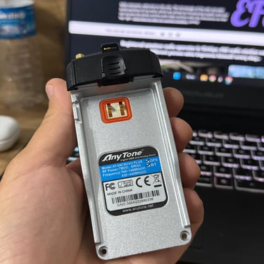
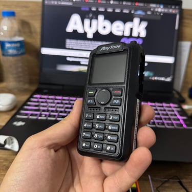
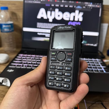
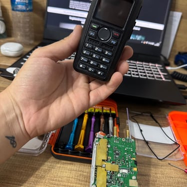
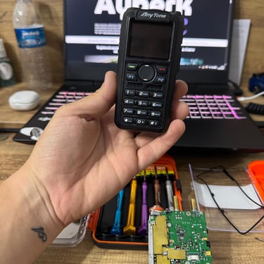
Anytone AT-D878UVII Plus
Internal Architecture and RF System Analysis
AYBERK BLOG
Anytone AT-D878UVII Plus
Introduction
The Anytone AT-D878UVII Plus is a dual-band (VHF/UHF) handheld transceiver supporting both Analog FM and DMR Tier II operation. Internally, the radio combines a classical superheterodyne RF architecture with modern DSP-based digital baseband processing. This hybrid approach results in a semi-SDR design that is optimized for low power consumption, high selectivity, and robust digital performance.
Unlike fully software-defined radios, the AT-D878UVII Plus preserves discrete RF filtering stages, analog intermediate-frequency (IF) processing, and hardware-assisted modulation. This design choice significantly improves adjacent-channel rejection, strong-signal handling capability, and overall RF robustness, particularly in congested RF environments.
Global System Architecture
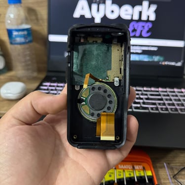
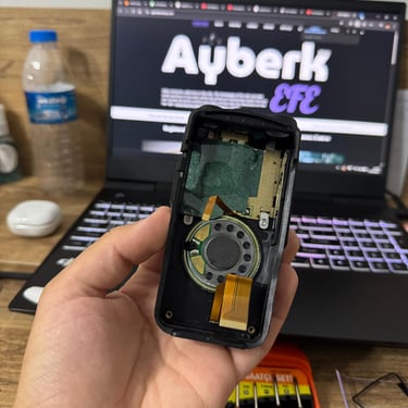
At a system level, the AT-D878UVII Plus follows a conventional superheterodyne signal flow. RF signals received at the 50-ohm antenna interface pass through a transmit/receive switching stage before entering band-specific filtering networks for VHF or UHF operation. After filtering, the signal is amplified by a low-noise amplifier (LNA) and then down-converted through a dual-conversion mixing architecture driven by a PLL-controlled VCO.
Following the first IF stage and associated SAW filtering, the signal undergoes a second frequency conversion to baseband, producing quadrature I/Q signals. These signals are digitized by an ADC and processed by the internal DSP, which performs demodulation, decoding, and audio processing. The recovered audio is then converted back to analog form and amplified to drive the internal speaker. The transmit chain mirrors this architecture in reverse, with the addition of RF power amplification and harmonic suppression stages.
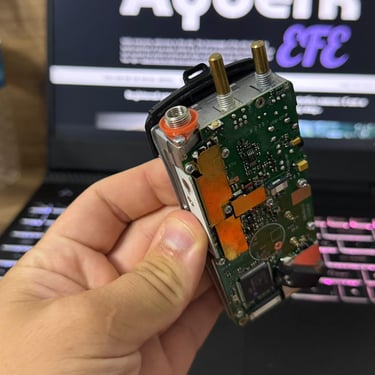
Antenna Interface and RF Front-End
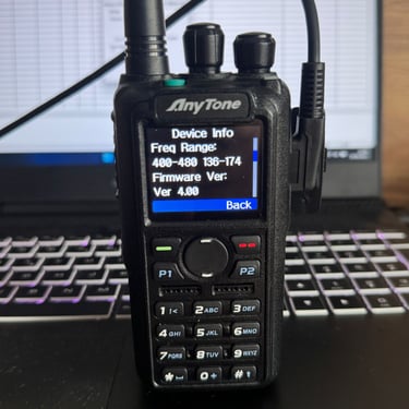
The radio employs an SMA-female antenna connector designed for a nominal 50-ohm impedance. A dual-band resonant matching network based on LC components ensures efficient power transfer and low VSWR across the 136–174 MHz VHF band and the 400–480 MHz UHF band.
RF switching between transmit and receive paths is achieved using PIN diodes or RF MOSFETs, providing approximately 60 dB of isolation during transmission. This isolation protects the receiver front-end from high transmit power levels and prevents receiver desensitization. Independent band-pass filters for VHF and UHF operation, implemented using a combination of LC networks and SAW filters, provide strong out-of-band rejection and minimize intermodulation effects in high-signal-density environments.
Low-Noise Amplifier (LNA)
The low-noise amplifier is a critical element of the receiver chain and largely defines the radio’s sensitivity and dynamic range. The LNA typically exhibits a noise figure in the range of approximately 1.2 to 1.8 dB, with a gain of 12 to 18 dB. Biasing of the LNA is controlled by the main MCU, allowing it to be disabled or operated at reduced power in battery-saving modes.
Frequency Synthesis, PLL, and Clocking
Frequency generation within the AT-D878UVII Plus is based on a temperature-compensated crystal oscillator (TCXO) with a typical stability of ±2.5 ppm. The reference frequency is commonly 12.8 MHz or 26 MHz. The stability and phase noise performance of this reference directly influence DMR bit-error rate and overall modulation quality.
A fractional-N PLL synthesizer provides fine frequency resolution, typically better than 1 kHz. The design uses a shared PLL architecture with separate VHF and UHF VCO tanks. The PLL output passes through a loop filter and RF buffer stages before driving the mixers. Low phase noise in this subsystem is essential for clean 4-FSK modulation and minimal adjacent-channel interference.
Receiver Chain
In the receiver path, incoming RF signals are first down-converted to a high first IF, typically in the range of 45 to 70 MHz. This choice improves image rejection and selectivity. The first IF signal is then passed through a SAW filter, with bandwidths of approximately 15 kHz for wideband analog FM and around 7.5 kHz for digital operation.
A second frequency conversion brings the signal down to baseband, producing quadrature I/Q outputs. These baseband signals are suitable for high-precision digital processing and are forwarded to the ADC and DSP stages.
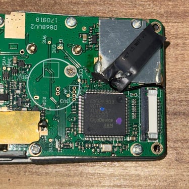
ADC and Digital Signal Processing
The analog-to-digital conversion stage typically uses a resolution of 12 to 14 bits, with sampling rates in the range of approximately 48 to 96 kHz. The ADC samples the I/Q baseband signals, which are then processed by the DSP core.
The DSP is responsible for both analog and digital demodulation tasks, including FM demodulation, 4-FSK demodulation, symbol timing recovery, carrier recovery, frame synchronization, and error correction. As such, it forms the computational heart of the receiver and transmitter signal paths.
DMR Baseband Processing
At the physical layer, DMR operation uses 4-FSK modulation with a symbol rate of 4800 baud and a channel spacing of 12.5 kHz. The system employs two-slot TDMA, with each time slot occupying 30 ms.
DMR frames consist of voice bursts, embedded signaling, synchronization patterns, and control information such as color codes and talkgroup identifiers. Forward error correction, interleaving, and CRC validation are used to maintain intelligible audio even at bit-error rates approaching approximately five percent.
Voice Codec and Audio Pipeline
Voice encoding and decoding are performed using the AMBE+2 codec, with a net voice bit rate of approximately 2450 bps. In the receive path, decoded digital voice data is converted to analog audio via a DAC and amplified to drive the internal speaker. In the transmit path, microphone audio is digitized, processed by AGC, encoded by the AMBE codec, and then modulated as a 4-FSK digital signal before being passed to the RF transmitter chain.
Transmitter Chain
For analog operation, the radio employs direct FM modulation. In digital mode, baseband-generated 4-FSK modulation is applied to the VCO. The RF power amplifier stage is typically based on MOSFET technology and provides selectable output power levels of approximately 7 W (high), 3 to 4 W (medium), and around 1 W (low).
Harmonic suppression is achieved using a multi-stage low-pass filter, typically of approximately seventh order, ensuring spurious emissions remain below −36 dBm.
MCU, Firmware, and Peripheral Control
The main MCU manages the user interface, TFT display control, CPS communication, and memory operations. Peripheral modules such as GPS, Bluetooth, and APRS functionality are connected via UART or SPI interfaces. An RTOS-like task scheduler is likely employed to coordinate time-critical DSP tasks alongside user interface and background system operations.
Power Management System
The radio is powered by a two-cell lithium-ion battery pack with a nominal voltage of approximately 7.4 V and a capacity of around 3100 mAh. Power regulation is handled by buck converters for high-current loads such as the RF power amplifier, and low-noise LDO regulators for sensitive DSP and ADC circuitry. Analog and digital ground planes are separated to minimize noise coupling.
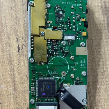
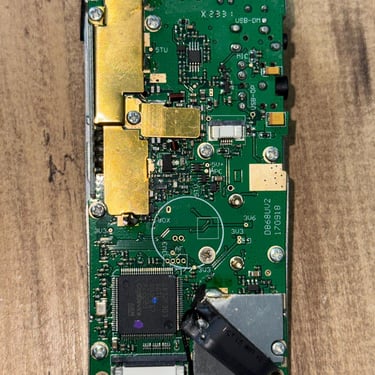
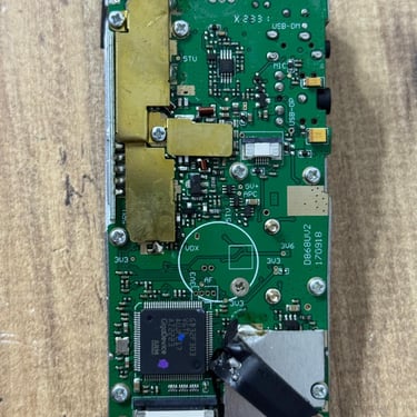
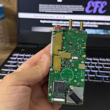
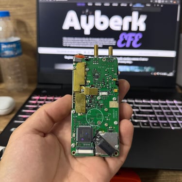
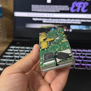
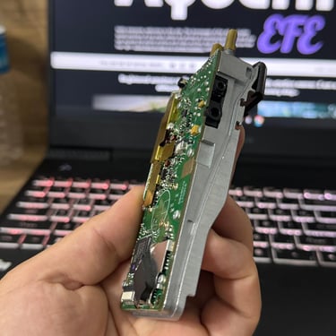
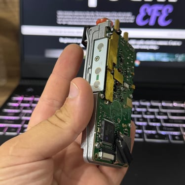
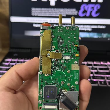
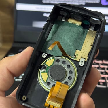
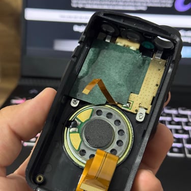
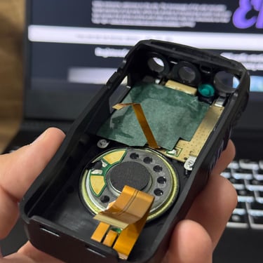
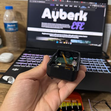
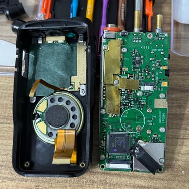
PCB Layout and RF Design Considerations
Internally, the radio uses a multi-layer PCB with clear separation between RF, digital, and power sections. Controlled-impedance RF traces, shielded RF compartments, and dense ground stitching vias around IF and PLL sections are employed to ensure RF stability and minimize interference.
Service, Debug, and Measurement Perspective
Key diagnostic test points include PLL lock detection, IF1 and IF2 outputs, audio DAC output, and RF directional couplers. Typical failure modes include PLL unlock conditions resulting in loss of transmit capability, LNA bias failures leading to reduced sensitivity, and PA MOSFET degradation causing reduced output power.
Engineering Evaluation and Conclusion
The Anytone AT-D878UVII Plus represents a highly optimized hybrid RF/DSP architecture that successfully balances traditional RF robustness with modern digital flexibility. Its excellent PLL stability, strong adjacent-channel rejection, reliable DMR implementation, and efficient power management allow it to deliver near-professional RF performance within its class and price range.
Rather than being merely a consumer-grade DMR handheld, the AT-D878UVII Plus is a carefully engineered RF system that reflects many of the design principles found in professional radio equipment, making it an excellent platform for both advanced operation and technical study.